How Long Does It Take to Manufacture a PCB?
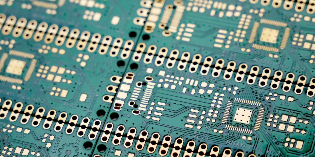
The time required to manufacture a printed circuit board (PCB) varies depending on factors such as complexity, materials, order quantity, and manufacturing processes. This article provides a detailed breakdown of the PCB production timeline, supported by research and statistics.
1. Average PCB Manufacturing Time
The typical manufacturing time for standard PCBs ranges from 3 to 15 working days, depending on the complexity and production scale:
- Simple 1-2 Layer PCBs: These can be produced in as little as 24 hours for small prototypes or up to 3-5 days for larger batches.
- Multilayer PCBs (4-6 Layers): Production time increases to around 5-8 days due to the additional lamination cycles and routing complexities.
- Advanced PCBs (HDI or 10+ Layers): These can take 10-20 days, depending on the inclusion of features like blind/buried vias or heavy copper layers.
For urgent needs, manufacturers like OurPCB offer expedited services, completing some orders within 24-48 hours.
2. Key Stages in PCB Manufacturing
PCB manufacturing involves several steps, each contributing to the total lead time:
- Order Review and Design Validation: Manufacturers review Gerber files and ensure all design specifications are correct.
- Material Preparation: Copper-clad laminates are prepared based on board thickness and layer requirements.
- Imaging and Etching: Circuit patterns are transferred onto the board using photolithography, followed by etching to remove excess copper.
- Lamination for Multilayer Boards: Multilayer boards require multiple lamination cycles, especially if blind or buried vias are involved.
- Drilling and Plating: Holes are drilled and plated for electrical connectivity.
- Solder Mask and Silkscreen Application: Protective layers and markings are applied.
- Quality Testing: Electrical tests ensure functionality before packaging.
3. Factors Affecting Manufacturing Time
Several variables influence how long it takes to produce a PCB:
- Design Complexity: High-density designs with multiple layers or advanced features like HDI routing require more time.
- Order Quantity: Prototypes take less time than large-scale production runs due to reduced setup requirements.
- Material Availability: Delays in sourcing specialized materials like heavy copper or flexible substrates can extend lead times.
- Testing Requirements: Advanced quality control measures, such as impedance testing or environmental stress screening, add extra time.
4. Expedited Manufacturing Options
For projects with tight deadlines, quick-turn services can significantly reduce lead times:
- Some manufacturers offer 24-hour turnaround for simple PCBs.
- Advanced boards with higher layer counts can be expedited within 3-5 days.
5. Statistical Insights
- The global average lead time for standard PCBs is around 7-10 working days for medium complexity designs.
- Quick-turn prototypes account for a growing segment of the industry, with demand driven by rapid product development cycles in sectors like IoT and consumer electronics.
- Multilayer PCBs dominate the market, representing a significant portion of global PCB production due to their application in compact devices.
6. Tips to Minimize Lead Times
To reduce manufacturing times:
- Use Design for Manufacturability (DFM) Principles: Simplify layouts to avoid unnecessary complexities that can delay production.
- Partner with Reliable Manufacturers: Collaborate with trusted manufacturers
- Plan Ahead: Ensure all design files are complete and error-free before submission to prevent delays caused by revisions or corrections.


